LET'S TALK
Miniaturization (iNPACK) - Organic Substrates & Advanced IC Packaging Solutions
Explore Solutions
Industry 4.0 / 5.0

Strategic Capabilities for Aerospace & Aviation PCBs

HDI & Miniaturization Technologies

High-Reliability, High-Quality PCBs - Prototype to Low/Mid Production Volumes

HDI, Rigid/Rigid-Flex, RF Boards, Heat Management Solutions & More

Self-driving Technology Rides on High Reliability, High-Performance Execution Enabled by PCBs

Advanced Communications Systems Depend on High-Reliability PCBs

High-Power PCBs for Energy Industries
Our highly experienced engineering team is at your service – from design to fabrication for an All-in-One solution
Our sales team will be happy to provide you with a quote. Simply send us an email detailing your requirements and we’ll reply ASAP
We provide a wide range of PCB Assembly Services for various products and industries based on cutting-edge automation and processes including POP – Package on Package, 01/005 Components, Micro BGAs, Flexible PCBs, Multi-Layered Prints, and more. Our services span from PCBA Assembly and mechanical assembly through integration and ICT,J-TAG, and final testing of PCBA, complete systems, and products. Also available – Acrylic coating by a fully automatic machine, Potting, Ultrasonic soldering, and DfM.
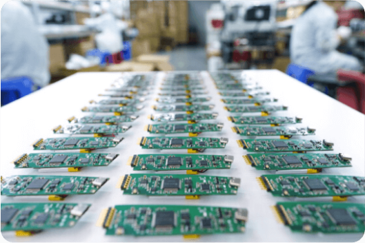
Whether you need a low volume or a high volume of PCBs, you’ll always receive the same high standards of quality from our certified manufacturing facility (ISO9001/ISO14001/ISO13485). All PCB Technologies solutions are assembled by certified experts (IPC-A-610 and J-STD-001.
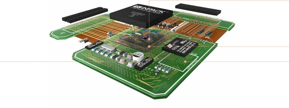
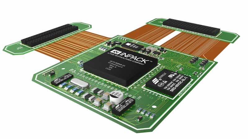
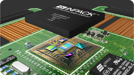
Advanced System-in-Package (SiP) solutions are multi-component, multifunction products that leverage PCB Technologies’ core strengths in order to offer our customers higher levels of miniaturized integration with reduced lead times. These include:
We offer a high-efficiency All-in-One Solution, resulting in brighter ideas and better-quality products at significantly shorter lead times. Our advanced R&D center, located within the same large complex as our manufacturing facilities, allows for the seamless creation of custom SiP; from design to manufacture, assembly, and testing.
An entire suite of Design for Manufacturing (DfM) services that expertly analyze PCB designs with the aim of improving quality, yields, and delivery times while also reducing costs.
Design for Testability (DfT) services help to identify possible snags with PCB designs before starting mass production, minimizing defects while maximizing reliability and repeatability.
The In-Circuit Test (ICT) can pinpoint defects in the board from the assembly process, such as component mismatches, misplacements, or missing components. PCB Technologies also delivers functionality tests, whereby PCBs are tested in their final production environment to ensure proper functionality according to specs.
Our Value Analysis/Value Engineering (VA/VE) solutions enable customers to gain the maximum value from their PCB designs. Unlocking greater product value through continuous improvements is facilitated by combining our services: Design for Manufacturing (DfM), Design for Testability (DfT), Design for Procurement (DfP), Design for Cost (DfC), and Design for Assembly (DfA).
PCB Technologies works hand-in-hand with customers not only to improve existing PCB designs but also to support clients’ new product designs, from launch through scaling-up production and long-term management.
With a long history of cutting-edge PCB design expertise, coupled with top-tier production capabilities, our customers rely exclusively on PCB Technologies for their PCB Full Turnkey projects.
We utilize the latest technologies and automation equipment to create high-quality production processes; tailored to the product requirements. Solutions involve all aspects of assembly — efficiently transforming part integration, cabling, and electronics, into modules or end products. Customers also benefit from our broad market purchasing power in sourcing the best components at cost-effective prices.
Frequently Asked Questions
What services does PCB Technologies offer?
PCB Technologies provides comprehensive solutions encompassing PCB fabrication, PCB assembly (PCBA), and advanced miniaturization through our iNPACK platform. Our services include supply chain management, assembly, testing, inspection, rework, and New Product Introduction (NPI).
Which industries does PCB Technologies serve?
We cater to a diverse range of industries, including aerospace, defense, automotive, medical electronics, communications, semiconductor, consumer electronics, and energy sectors. Our solutions are tailored to meet the specific needs of each industry, ensuring high reliability and performance.
What is iNPACK, and how does it benefit my designs?
iNPACK is our advanced IC packaging and miniaturization solution that integrates organic substrates and System-in-Package (SiP) technologies. It enables size reduction, enhanced thermal conductivity, and improved signal integrity, making it ideal for compact and high-performance electronic devices.
Can you handle both prototype and mass production?
Yes, we support projects from prototype to low and mid-volume production. Our flexible manufacturing capabilities ensure that we can scale production to meet your specific requirements, maintaining high quality and efficiency throughout.
What quality standards does PCB Technologies adhere to?
We are committed to delivering products that meet the highest industry standards. Our certifications include ISO 9001, ISO 14001, ISO 13485, and AS 9100. Our Quality Control staff are trained and certified in IPC Class 2 and 3, ensuring consistent quality and compliance across all our manufacturing processes.
Do you offer design support services?
Absolutely. Our experienced engineering team provides Design for Manufacturing (DfM) and Design for Assembly (DfA) services and also design support in the IC packaging segment, offering valuable insights to optimize your designs for manufacturability and cost-effectiveness.
What is your approach to thermal management in PCBs?
We employ advanced thermal management solutions, including embedded coins, via farms, heat sink integration, thick copper, controlled CTE materials, and optimized stack-ups, to ensure effective heat dissipation in high-power applications.
How do you ensure the timely delivery of projects?
Our global manufacturing network, coupled with efficient logistics and project management, allows us to meet tight deadlines and deliver products on time, even for complex and custom designs.
Can you assist with New Product Introduction (NPI)?
Yes, we offer comprehensive NPI services, guiding your product from concept through prototyping to full-scale production. Our team works closely with you to ensure a smooth transition and successful market entry.
articles
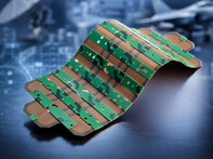
The electronics industry is rapidly moving toward smaller, lighter, faster, and more reliable products. From aerospace systems and medical instrumentation to defense electronics, automotive controls, industrial automation, RF communication, and wearable technology, modern electronic products demand interconnect solutions that traditional rigid PCBs alone often cannot provide. This is where flex and rigid-flex PCB technology has become one of the most important enabling technologies in advanced electronic design.
articles
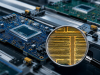
As electronic systems continue shrinking in size while expanding in performance, traditional PCB architectures are approaching their physical and electrical limitations.
events
Meet us at IMS 2026
9-12 of June, 2026
We will contact you shortly