Organic QFN IC Packages: Comparing Packaging Options QFN, LGA & Materials

Yaniv Maydar
|28th August ,2024
PART TWO of our three-part QFN blog series:
Amid the rapid IC packaging evolution, many different package types have emerged, each embodying its own distinct set of characteristics, advantages and challenges. Differing IC package types can be distinguished by variations in mounting style, pin layout, shape and pin count. Engineers and designers must fully grasp these differences in order to select the most advantageous IC package type for their specific application.
Main Characteristics of QFN (Quad Flat No-leads) & LGA (Land Grid Array)
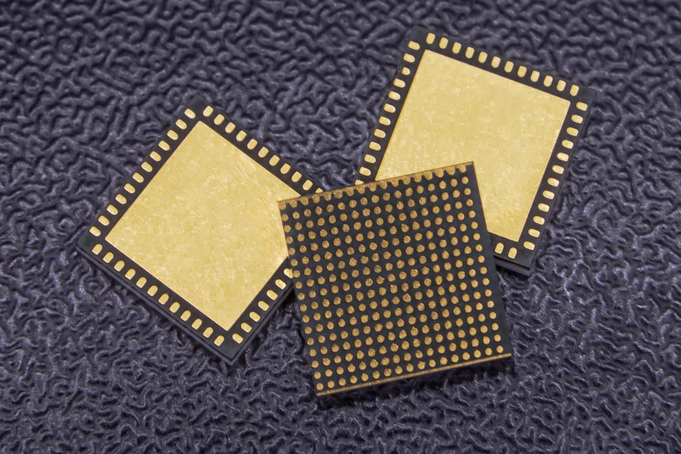
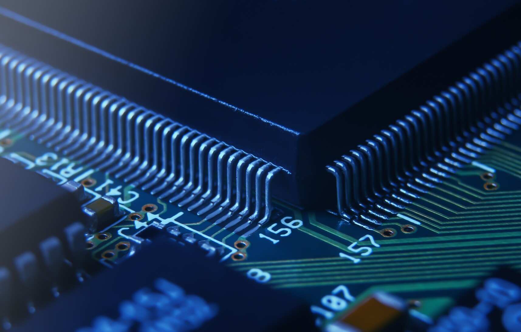
QFN (Quad Flat No-leads):
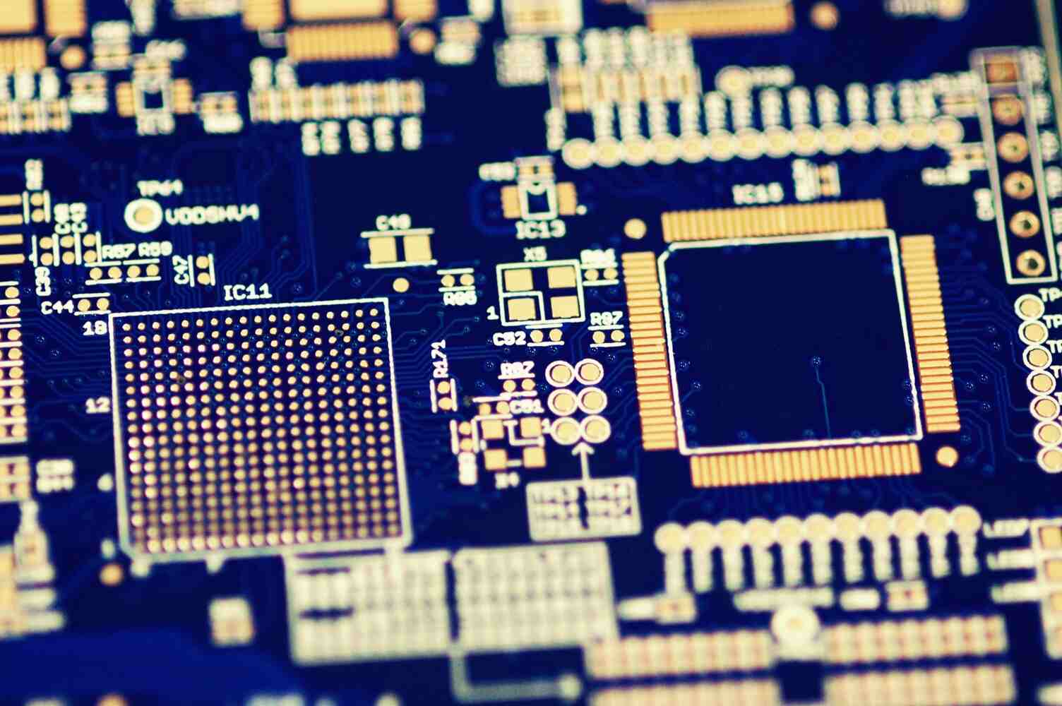
- Package Design: QFN packages have exposed pads on the bottom surface of the package, typically arranged in a grid pattern. Leads are absent, which contributes to their compact size and low profile.
- Soldering: QFN packages are soldered directly onto the surface of the PCB, with the exposed thermal pad underneath aiding in heat dissipation. They require careful soldering techniques, such as reflow soldering, to ensure proper connection and alignment.
- Size: QFN packages are generally smaller than equivalent LGA packages due to their flat, leadless design. This makes them suitable for applications where space-saving is crucial.
- Electrical Performance: QFN packages typically offer good electrical performance, with shorter lead lengths and reduced parasitic inductance and capacitance compared to some other package types.
- Applications: QFN packages are commonly used in consumer electronics, telecommunications, and other applications where space, cost, and thermal management are important considerations.
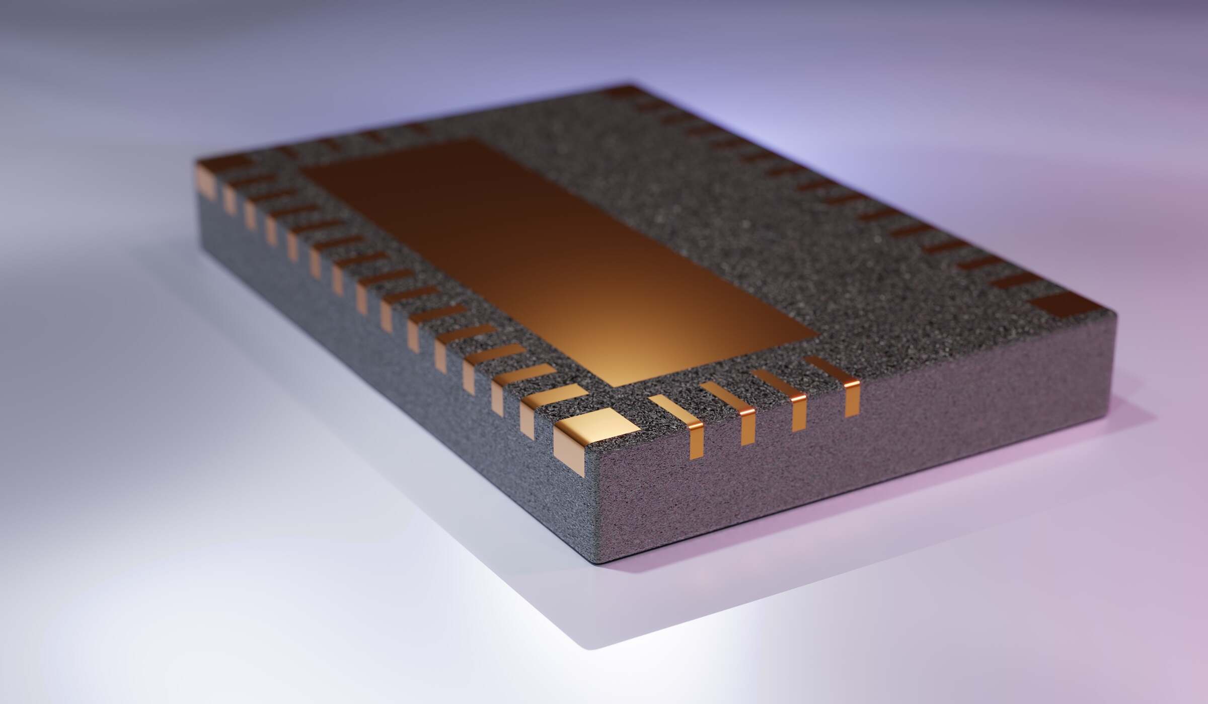
LGA (Land Grid Array):
- Package Design: LGA packages have an array of pads on the underside of the package, but unlike QFN, these pads are typically arranged in a regular grid with no leads extending out from the sides of the package.
- Soldering: LGA packages also require reflow soldering but do not have the issue of exposed leads, simplifying the soldering process. A lack of leads may also reduce the risk of mechanical stress during thermal cycling.
- Size: LGA packages tend to be larger than QFN packages due to its grid array design and the need for sufficient space between pads for soldering and thermal considerations.
- Electrical Performance: LGA packages can offer outstanding electrical performance, often better than QFN packages, especially for high-frequency applications, due to shorter path-lengths and reduced parasitic effects.
- Applications: LGA packages are generally found in applications for high-speed data transfer, such as high-performance computing, servers or networking equipment, where signal integrity and thermal management are paramount.
QFN & LGA Packaging Features
Depending upon application requirements, such as size constraints, thermal management needs, specific demands in electrical performance and cost considerations, each packaging method offers its own distinct advantages.
|
Features |
Description |
|
Size & Profile |
QFN packages are typically smaller with a lower profile compared to LGA packages. |
|
Thermal Management |
QFN packages often have an exposed thermal pad underneath, better supporting heat dissipation, while LGA packages rely on thermal performance of the PCB pad area alone. |
|
Cost |
QFN packages are generally more cost-effective due to a simpler design and smaller size. |
|
Assembly & Reliability |
Both QFN & LGA packages require precise soldering techniques, however QFN packages may involve challenges during inspection, due to exposed leads. |
QFN Material Types
QFN (Quad Flat No-leads) packages come in different material types. Although there are many determining factors influencing the selection of materials for QFN packages, generally, the material can function to provide mechanical support, aid in heat dissipation and assist manufacturability. Each material type should be examined carefully to reveal the important advantages and considerations related to the application at hand:
3 Types: Ceramic / Organic / Lead Frame
- Ceramic QFN:
- Material: Ceramic QFN packages are made from ceramic materials, which provide higher thermal conductivity compared to organic materials.
- Advantages:
- Thermal Performance: Ceramic has excellent thermal conductivity, making ceramic QFNs well-suited for high-power applications where effective heat dissipation is crucial.
- Reliability: Ceramic materials typically offer better mechanical strength and reliability compared to organic materials, making them more resistant to mechanical stress and thermal cycling.
- High-Frequency Applications: Ceramic QFNs can maintain stable electrical characteristics at high frequencies due to their low dielectric constant and minimal signal loss.
- Considerations:
- Cost: Ceramic QFN packages tend to be more expensive than their organic counterparts due to the higher cost of ceramic materials and manufacturing processes.
- Manufacturability: Ceramic packages may require specialized manufacturing techniques, which can create a more complex production process.
- Organic QFN:
- Material: Organic QFN packages are made from organic materials, such as epoxy or laminate substrates.
- Advantages:
- Cost: Organic QFN packages are generally more cost-effective compared with ceramic versions. Compatibility: Compatible with standard PCB manufacturing processes and equipment, simplifying production.
- Weight: Organic packages are lighter than ceramic, a distinct advantage in weight-sensitive applications.
- Considerations:
- Thermal Performance: Organic materials exhibit lower thermal conductivity compared to ceramics, which may limit their use in high-power / high-temperature applications.
- Mechanical Strength: Organic materials may have a lower mechanical strength than ceramics, and can be more susceptible to mechanical stress damage compared to ceramics.
- Lead Frame QFN:
- Material: Lead frame QFN packages use a metal lead frame, typically made from copper or alloy, with the die attached, and wire bonded to the leads.
- Advantages:
- Cost: Lead frame QFN packages are often the most cost-effective option of all three package types.
- Reliability: Lead frames provide robust mechanical strength and stability, making them suitable for a wider range of applications.
- Ease of Assembly: Lead frame packages are relatively straightforward to assemble and handle during the manufacturing process.
- Considerations:
- Thermal Performance: Lead frame packages may be limited in thermal conductivity compared to ceramic versions, depending on the specific design and materials used.
- Size: Lead frame packages tend to be larger compared to ceramic or organic versions due to the structure of the lead frame.
Overall Selection Considerations:
- Application Requirements: Take into account thermal management needs, electrical performance requirements, and mechanical stability and durability.
- Cost Constraints: Review the relative cost-effectiveness of each package type to determine if it’s a match with the budget.
- Manufacturability: Evaluate ease of manufacturing, assembly and test.
- Performance: Assess electrical characteristics such as signal integrity and high-frequency performance.
In Conclusion
The choice between ceramic, organic, or lead frame QFN packages will require a careful balanced approach, weighing up numerous factors; such as thermal performance, cost, manufacturability, reliability etc., and how that compares with the requirements of a specific project or application. Each package type offers distinct advantages and considerations that should be evaluated during the design phase.
FYI: Other QFN Names/ Types :
QFN packaging can be referred to by different names:
- QFN – quad flat no-lead package
- SQFN- standard QFN
- TQFN- Thin QFN
- MLF – micro-lead-frame
- MQFN- Micro QFN
- MLPD – micro-lead-frame package dual
- MLPM – micro-lead-frame package micro
- MLPQ – micro-lead-frame package quad
- UQFN- Ultra Thin QFN
- LQFN-Leadless QFN
- RQFN- Ruggedized QFN
- DRQFN- Dual Row QFN
- VQFN – very thin quad flat no-lead
- EQFN- Extended QFN
- DFN – dual flat no-lead package
- LQFP- Low-profile Quad Flat Package
This concludes PART TWO of our three-part blog series: We hope you’ve found it useful.
Don’t miss PART THREE: The FINAL segment in this series will explore advanced QFN technologies and testing, panel-level assembly and near hermetic sealing + new innovations and customization in QFN packaging.
About iNPACK
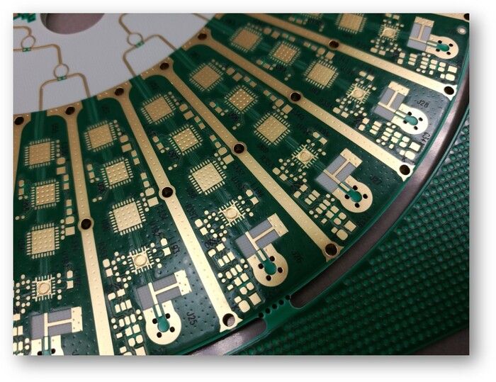
At iNPACK (a PCB Technologies Company), we provide IC packages in a complex array of shapes, sizes, and materials, giving you the ability to select the exact features and functionality best suited to your specific application. This determination however is dependent upon a number of factors, including: Pitch, Dimensions, Lead Count, Thermal Requirements, Costing and more.
The QFN (Quad Flat No Lead), represents a specific IC Packaging solution. iNPACK offers a customized panel-level solution featuring a plastic-encapsulated laminate panel, with a variety of dielectric and CTE options for electrical interconnection with the PCB. This type of packaging can be offered as a full turn-key solution, (including assembly and testing), or as a stand-alone substrate, combined with a cavity lid.