Advanced QFN Technologies – Panel-Level Assembly, Near-Hermetic Sealing & Testing

Yaniv Maydar
|4th September ,2024
PART THREE of our three-part series:
This Final Segment Focuses on:
Advanced QFN Technologies - Panel-Level Assembly, Near-Hermetic Sealing & Testing
An important aspect of advanced packaging technologies involves principles of Design-For-Manufacturing (DFM); a system that aims to ensure IC packages can be manufactured efficiently and reliably, with a view towards higher yields and lower costs. In the case of QFN package fabrication, DFM requires examining assembly options, sealing methods and testing processes.
SEALING METHODS
iNPACK QFN – Prepreg Sealing, Proprietary Process: Prepregs, (pre-impregnated materials), offer several advantages over many other types of adhesives or bonding materials, particularly in the context of electronics manufacturing and PCB assembly:
- Controlled Resin Content:
- Prepregs are manufactured with a controlled amount of resin impregnated into the reinforcing fibers (typically fiberglass). A controlled resin content ensures consistent and predictable adhesive properties during assembly and lamination processes.
- Consistent Thickness:
- Prepregs are available in various thicknesses and are manufactured with consistent thickness tolerances. This uniformity helps maintain consistent bonding and insulation properties across the PCB during lamination.
- Adhesive & Insulation Properties:
- Prepregs provide excellent adhesive properties, bonding tightly to copper layers and other materials during the lamination process. They offer insulation between conductive layers, preventing electrical shorts and ensuring reliability of the PCB.
- Mechanical Strength:
- Reinforcing fibers within prepregs (usually fiberglass) contribute to mechanical strength, which enhances the structural integrity of the PCB, providing robust barrier against mechanical stresses and vibrations.
- Near-Hermetic Sealing:
- Using prepregs as a sealing process can help guard against fine and gross leaks.
- Thermal Stability:
- Prepregs are designed to withstand high temperatures during the PCB lamination process (typically around 175-200°C). They maintain their adhesive and mechanical properties under thermal stress, ensuring reliable performance in high-temperature environments.
- Compatibility with Manufacturing Processes:
- Prepregs are compatible with standard PCB manufacturing processes such as lamination and soldering. They integrate seamlessly into automated assembly lines, for smooth, efficient, cost-effective production.
- Environmental Considerations:
- Many prepregs are formulated to meet environmental regulations and industry standards for sustainability and safety. They are often halogen-free and comply with RoHS (Restriction of Hazardous Substances) directives.
- Versatility:
- Prepregs come in many types and formulations, suitable for different PCB designs and requirements. This versatility allows designers to choose prepregs with specific properties, such as high Tg (Glass Transition Temperature) for increased thermal stability, or low Dk (Dielectric Constant) for improved signal integrity.
In Conclusion: Prepregs offer advantages over other adhesives primarily due to their controlled resin content, consistent thickness, excellent adhesive and insulation properties, mechanical strength, thermal stability, compatibility with manufacturing processes, environmental compliance, and versatility in meeting diverse PCB design needs. These characteristics make prepregs a popular choice in the electronics industry to ensure reliable and high-performance PCB assemblies.
- B-Stage Epoxy Near-Hermetic Sealing: B-stage epoxy is a reference to an intermediate curing process stage in epoxy resin, where it is partially cured or partially cross-linked. B-stage epoxy resins offer numerous advantages in IC package sealing, described in the following:
-
- Controlled Curing Process:
- B-stage epoxy resins allow for a controlled curing process. It remains in a semi-solid state until exposed to elevated temperatures, or specific curing conditions. This controlled curing ability enables precise timing and precise manipulation during the sealing process.
- Adhesive and Sealing Properties:
- B-stage epoxy resins have excellent adhesive properties, capable of forming strong bonds between different materials used in IC packaging, such as metals, ceramics, and plastics. They are effective in sealing against moisture and contaminants, crucial for protecting semiconductor components.
- Compatibility with Assembly Processes:
- B-stage epoxy can be applied as a liquid or film during initial stages of IC packaging assembly. This flexibility allows for easier handling and application before the final curing stage. It can be dispensed or coated onto substrates, components, or other areas that require sealing; enabling efficient manufacturing.
- Thermal & Chemical Stability:
- Once fully cured, epoxy resins exhibit excellent thermal and chemical stability. They withstand high temperatures and resist degradation from chemicals. This ensures long-term reliability and performance of sealed IC packages for a wide range of operating environments.
- Reduced Stress & Warpage:
- B-stage epoxy resins typically undergo controlled shrinkage during the final curing process, which minimizes stress and warpage in the sealed IC package. This is crucial in maintaining dimensional stability and preventing mechanical failure in packaged semiconductor devices.
- Moisture Protection:
- Effective moisture protection is critical in IC packaging to prevent corrosion, electrical malfunctions, and reliability issues. B-stage epoxy resins provide a reliable barrier against moisture ingress, enhancing both lifespan and performance of semiconductor devices.
- Cost-Effectiveness:
- Using B-stage epoxy resins can contribute to cost savings in IC packaging assembly, allowing for efficient application and curing processes, that can reduce labor and material costs associated with sealing operations.
- Controlled Curing Process:
In Conclusion: B-stage epoxy resins offer significant advantages in IC packaging sealing: controlled curing, excellent adhesive properties, compatibility with assembly processes, thermal and chemical stability, stress reduction, moisture protection, and cost-effectiveness. These characteristics make B-stage epoxy resins a preferred choice for reliability, longevity, and high performance, in the fabrication of semiconductor devices for a wide variety of applications.

PANEL LEVEL ASSEMBLY (PLA) & SEALING PROCESS BY iNPACK
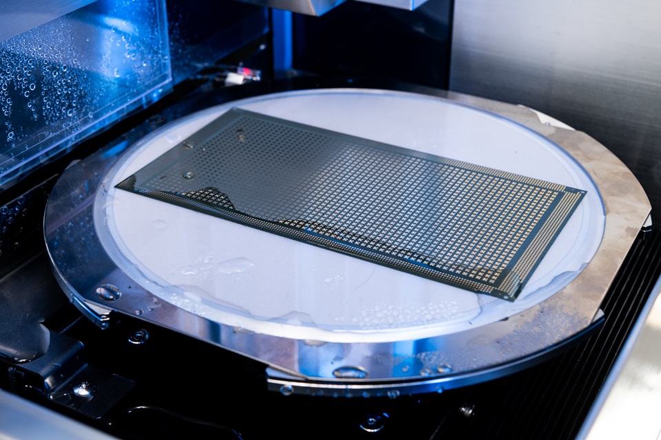
iNPACK perform Panel-level IC assembly (PLA), where multiple ICs are fabricated and assembled simultaneously on a larger substrate known as a panel, rather than individually on smaller wafers. iNPACK has also developed a panel-to-panel sealing method, based on prepregs and B-stage epoxy, to achieve near-hermetic sealing packaging qualities.
Advantages & Disadvantages of PLA:
|
Issue |
PROs |
Issue |
CONs |
|
Cost Efficiency |
PLA economizes on scale by processing multiple ICs in parallel on a single large substrate – reducing per-unit manufacturing costs compared to wafer-level or individual die-level assembly. |
Complex Handling & Processing |
PLA involves handling larger, more complex substrates, which can require specialized equipment and infrastructure, which may increase initial setup costs and operational complexity. |
|
Maximized Throughput |
PLA assembly of multiple ICs simultaneously on a single large panel, allows for higher production throughput compared to sequential processing of individual dies or wafers, resulting in faster TTM for products. |
Increased Defect Rates |
The larger scale of PLA can create issues with uniformity and consistency across all ICs on the panel, requiring careful management of process variations to mitigate defects. |
|
Less Handling Damage |
PLA processes can reduce handling damage during assembly due to fewer individual ICs or dies being handled / processed separately. This improves overall yield and minimizes manufacturing defects. |
Application Limitations |
PLA may be better suited for certain types of ICs or applications where high-volume production and cost efficiency outweigh the complexities and potential drawbacks related to panel-level processing. |
|
Improved Yield |
PLA potentially improves yield rates by allowing defects in individual ICs or dies to be identified and managed earlier in the manufacturing process, well before final assembly and packaging. |
Design & Layout Constraints |
Designing IC layouts for PLA requires careful consideration of panel size, spacing, plus alignment constraints. Design modifications may be necessary to optimize both yield & performance. |
|
Flexible Design & Integration |
PLA offers flexibility for integrating different IC designs / configurations on the same panel. This flexibility better supports customization and is well adapted to meeting individual customer requirements. |
Quality Control Challenges |
Ensuring uniform quality and reliability across all ICs on a panel can be challenging. Effective quality control measures & testing protocols are critical to mitigate risks associated with batch processing. |
|
Advanced Packaging Technologies |
PLA allows adoption of advanced packaging methods i.e., fan-out wafer-level packaging (FOWLP) or system-in-package (SiP) solutions, for better integration / performance levels in semiconductor devices. |
|
|
In Conclusion: The suitability of PLA depends on specific manufacturing goals, product requirements, and the ability to manage and mitigate any associated risks.
SEALING & MOLDING PANEL-LEVEL
Near-Hermetic Sealing: As used in IC packaging, near-hermetic sealing refers to a sealing technique that provides a certain level of moisture protection and environmental isolation approaching that of hermetic sealing, but without attaining complete hermeticity. Hermetic sealing refers to a package that is completely impermeable to gases and moisture, typically achieved through metal seals and glass-to-metal seals. Near-hermetic sealing aims to minimize moisture and gas ingress into the IC package, to levels that are sufficient for the intended application, without requiring the complexity and cost associated with full hermetically sealed packages.
Key features & considerations of near-hermetic sealing include:
|
Features |
Description |
|
Materials & Construction |
Near-hermetic packages use materials and construction techniques that provide a high-level moisture barrier. Materials may incorporate advanced polymers or hybrid materials with low moisture permeability, as well as effective sealing methods around the package lid or seal. |
|
Seal Integrity |
The sealing process in near-hermetic packages is designed to maintain seal integrity over the expected lifetime of the device. This involves ensuring tight seals between the package lid or cover and the package body, to prevent moisture ingress. |
|
Moisture Protection |
Near-hermetic sealing aims to limit moisture ingress to levels that do not adversely affect the performance and reliability of the semiconductor device. This is critical for applications where moisture sensitivity is a concern, such as high-humidity environments or for long-term reliability. |
|
Environmental Considerations |
Near-hermetic sealing addresses environmental factors such as temperature variations and exposure to contaminants, in addition to moisture protection. The package design and materials are selected to provide adequate protection against these environmental hazards. |
|
Cost & Complexity |
Compared to fully hermetic packages, near-hermetic sealing is a more cost-effective solution, while still meeting stringent moisture protection requirements. Near-hermetic sealing doesn’t require the costly manufacturing associated with fully hermetic seals or the specialized equipment needed in their production and testing. |
|
Applications |
Near-hermetic sealing is suitable for a wide range of semiconductor applications where moderate moisture protection is sufficient and full hermeticity is not required. This includes consumer electronics, industrial sensors, automotive electronics, and medical devices to name a few. |

Near Hermetic Testing Methods: Testing near-hermetic IC packages involves assessing their resistance to moisture ingress (damp penetration) and their ability to maintain a stable internal environment over time. Common methods and considerations for testing near-hermetic IC packages are as follows:
- Visual Inspection:
- Conduct a visual inspection of the package for any signs of physical damage or sealing breaches. Check for potential compromise points to package integrity such as cracks, gaps, or delamination.
- Hermeticity Testing:
- Execute various hermeticity testing procedures to evaluate package sealing performance under various conditions. Common test methods include:
- Helium Leak Testing: Detects leaks by measuring the rate of helium gas escaping through potential breaches in the package.
- Bubble Testing: Packages are submerged in a liquid to check for gas bubbles, indicating leaks.
- Fine & Gross Leak Testing: Using specialized equipment to measure leak rates and to identify potential leaks.
- Moisture Sensitivity Level (MSL) Testing: Determines package moisture sensitivity levels using industry-standard tests such as JEDEC J-STD-020. It involves subjecting the package to specific temperature / humidity conditions, to check moisture absorption.
- Execute various hermeticity testing procedures to evaluate package sealing performance under various conditions. Common test methods include:
- Temperature Cycling:
- Subjects the IC package to temperature cycling tests that simulate real-world environmental conditions to measure reliability over time, accurately evaluating package responses to changes in temperature and potential moisture condensation.
- Highly Accelerated Stress Testing (HAST):
- A method of accelerated humidity testing by subjecting the package to extreme levels of temperature and humidity, invaluable in assessing package resistance to moisture-induced failures.
- Environmental Testing:
- Conduct environmental testing to simulate the conditions the IC package will encounter during its intended use. This may include exposure to temperature extremes, humidity, thermal shock, and vibration to evaluate overall reliability.
- Electrical Testing:
- Perform electrical tests both before and after environmental stress testing procedure to assess any changes in electrical performance due to moisture ingress or other environmental factors.
- Microscopic Examination:
- Microscopy techniques are used to examine internal structures and external surfaces for signs of corrosion, delamination, or other damage that may indicate moisture ingress.
- Accelerated Aging Tests:
- Subjects the IC package to accelerated aging processes to predict long-term reliability. This may include extended exposure to elevated temperatures and humidity conditions.
- Compliance Testing:
- Ensures that testing methods and results comply with relevant industry standards and customer specifications, such as JEDEC standards for moisture sensitivity and reliability testing.
In Conclusion: Testing near-hermetic IC packages entails carrying out a combination of many different rigorous testing methodologies and procedures in order to compile accurate performance data for this package type. Manufacturers and testing laboratories use these different methods routinely to verify that IC packages meet specific performance criteria and standards in providing robust protection against moisture and other environmental hazards.
This completes PART THREE of our three-part blog series: QFN IC Packages | Panel Level Process for Organic Types – iNPACK. We hope you’ve found it useful.
PLEASE FOLLOW OUR iNPACK PAGE for more in-depth blog articles, specifically designed to bring you quality IC Packaging Technology subject matter. WE’D LIKE TO HEAR FROM YOU…
Is there something in particular, you’d like to read about in our blogs?
About iNPACKTM
At iNPACK (a PCB Technologies subsidiary), we provide IC packages in a complex array of shapes, sizes, and materials, giving you the ability to select the exact features and functionality best suited to your specific application. This determination however is dependent upon a number of factors, including: Pitch, Dimensions, Lead Count, Thermal Requirements, Costing and more.
The QFN (Quad Flat No Lead), represents a specific IC Packaging solution. iNPACK offers a customized panel-level solution featuring a plastic-encapsulated laminate panel, with a variety of dielectric and CTE options for electrical interconnection with the PCB. This type of packaging can be offered as a full turn-key solution, (including assembly and testing), or as a stand-alone substrate, combined with a cavity lid.
Things You Should Know about iNPACK Processes:
- iNPACK develop and manufacture QFN, IC Packaging Solutions using a Panel Level Processes (PLA). This same process is applied to our LGA and BGA packaging solutions as well.
- The PLA process allows for optimal design and manufacturability, whereby our customers benefit from more cost-effective, high-performance, high-yield and high reliability IC Packaging Solutions.
- iNPACK can offer superior customized packaging solutions with a wide range of design options to choose from; embedded coins, hybrid construction substrates (for improved performance), multilayer QFN and many other advanced technologies.
Contact us anytime to ask questions or discuss your next project.


