HDI PCBs: HDI Boards – High Density Interconnect PCBs
Shlomi Danino
|11th January ,2025
The rollout of 5G & 6G networks has increased demand for high-performance, super-efficient electronic components. High-Density Interconnect (HDI) and High Speed PCBs, with their ability to integrate a far greater number of components within a much smaller footprint, are considered ‘Critical Components’ in the development of 5G & 6G infrastructure.
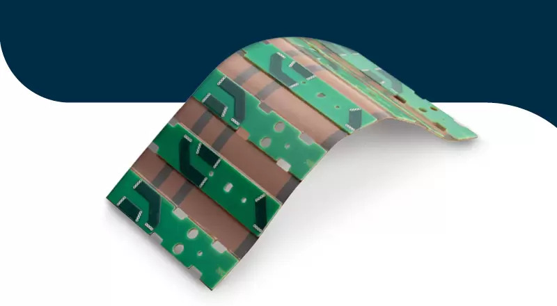
The rise of devices dependent upon HDI technology has swiftly grown to encompass a huge range of applications, such as telecommunications, consumer electronics, IoT, medical PCBs, automotive PCBs, wearables, and more.
1. Definition - What are HDI PCBs?
High-Density Interconnect PCBs are advanced circuit boards characterized by their higher wiring density per unit area compared to conventional PCBs. They utilize fine lines, smaller vias, and high-performance materials to enable complex, miniaturized electronic devices. HDI technology supports multiple layers, microvias, and sequential lamination, making it ideal for high-speed, high-frequency applications.
2. Benefits of HDI PCBs
-
- Miniaturization: Enables the production of smaller, lighter, and more compact devices.
- Improved Performance: Reduced signal loss and better electrical performance due to shorter interconnect paths.
- Higher Component Density: Supports more components in less space, essential for modern electronics.
- Enhanced Reliability: Lower thermal expansion, reducing stress and increasing durability.
- Cost Efficiency: Reduces the number of PCB layers required, leading to lower material costs.
3. Features of HDI PCBs
-
- Microvias: Smaller vias that improve routing density.
- Blind and Buried Vias: Allow for multi-layer connectivity without surface impact.
- Sequential Lamination: Provides multi-layer interconnections with higher precision.
- Thin Dielectric Layers: Enables better high-frequency signal transmission.
- Laser Drilling Technology: Ensures precision and uniformity in microvias.
4. Applications of HDI PCBs
HDI PCBs are widely used across industries due to their high reliability and advanced capabilities:
-
- Telecommunications: Found in 5G infrastructure, networking devices, and high-speed routers.
- Consumer Electronics: Used in smartphones, tablets, and wearables.
- Medical Devices: Applied in advanced imaging systems, pacemakers, and monitoring equipment.
- Automotive Industry: Integrated into ADAS (Advanced Driver Assistance Systems), navigation, and infotainment systems.
- Aerospace and Defense: Essential for avionics, military-grade electronics, and space applications.
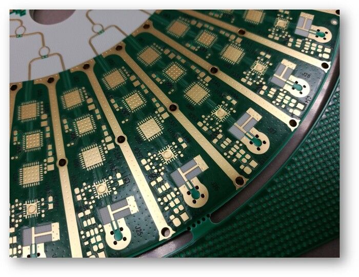
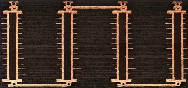
HDI PCBs
Sample 4-18, 10 mil drill buried Vias 3-16
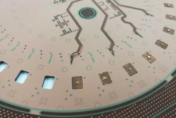
5. Technology and Production Process of HDI PCBs
The production of HDI PCBs involves several advanced PCB manufacturing processes:
-
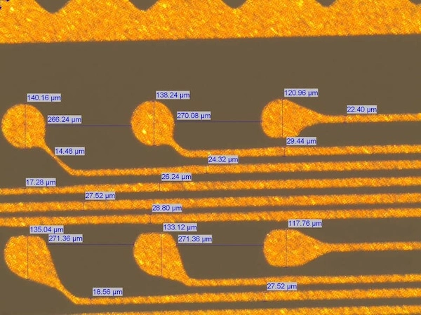
- Laser Drilling: Utilizes CO2 and UV lasers for precise via formation.
The ‘Excellon Cobra Hybrid Laser’ system, featuring both UV and IR (CO2) laser capabilities that cover a wide range of Flex and Rigid-flex circuit processing applications. Optimized Via drilling and profiling are achieved using a high-energy, short pulse width UV laser, combined with a super-pulsed CO2.
Clean, sharp ablation drilling enables a robust and uniform Via plating for electrical conductivity in (HDI).
-
- Sequential Lamination: Involves multiple lamination cycles to create high-layer count boards.
- Copper Deposition: Ensures strong and reliable electrical connections.
- High-Resolution Imaging: Used for fine-line and microvia patterning.
- Automated Optical Inspection (AOI): Verifies circuit accuracy and detects defects.
- Testing and Validation: Includes electrical testing, thermal cycling, and reliability assessments.
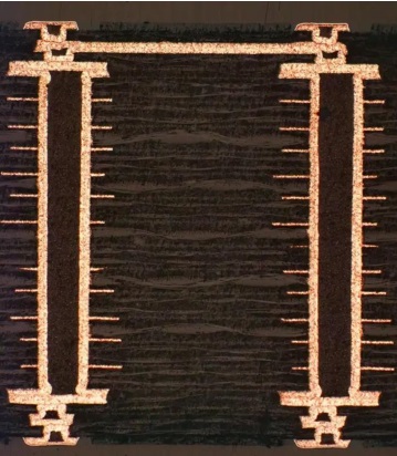
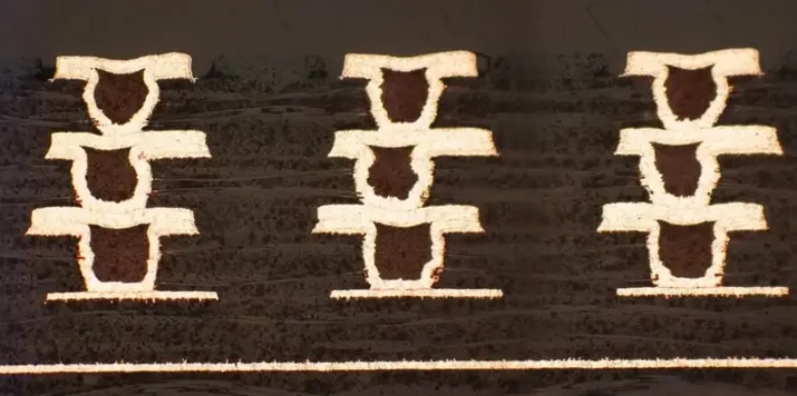
HDI 3 X sequential lamination X-axis cross-section, top row of stacked on buried Vias (10 mil drill)
HDI PCBs - The Future is Clear
As more devices are developed as a result of new technological trends, the need for higher complexity PCBs will also increase. What is considered cutting-edge today will very quickly become standard, and the focus will shift to on-boarding the next innovation as quickly as possible.
For that reason, technologically advanced PCB Manufacturers must be willing to support higher complexity; more layer builds, finer pitch, different materials, etc. This in turn leads to a very real and practical demand for new equipment, new raw materials, and the ability to take production to the next level.
As an adept PCB solutions provider, PCB Technologies is both agile and resourceful enough to meet each new technology and innovation that hits the market head-on. Whether in design, development, or production, we’re able to gear up with the most advanced machinery, sophisticated instrumentation, and complex processes to answer the needs of our customers for today and tomorrow.
Before you start your next project, contact one of our experts experienced in HDI, Rigid, Rigid-flex, IC packaging, and more. Find out how PCB Technologies can work for you
At PCB Technologies, we’re at the forefront of HDI PCB manufacturing, empowering next-gen devices with superior performance. Looking to optimize your next projects? Let’s talk! Connect with one of our experts today and discover how we can bring your vision to life