Flip Chip Vs. Wire Bonding Technology

Yaniv Maydar
|15th September ,2024
A Comprehensive Comparison of IC Packaging Interconnect Technologies
INTRODUCTION
When it comes to IC package interconnect selection, design engineers need to factor-in a host of complex issues, including cost, performance, end-use applications and much more. Two predominant technologies, Flip Chip and Wire Bonding, are popular interconnect options connecting ICs to packages or substrates.
Both bonding techniques play a crucial role in the fabrication and performance of electronic devices, while each presents its own unique advantages and challenges. This article compares in detail many critical factors influencing the selection of the optimal IC package interconnect option as it relates to a variety of different performance requirements.
MAIN CHARACTERISTICS:
|
Feature |
Wire Bonding |
Flip Chip |
|
General Description |
Wire Bonding is a long-standing and popular interconnection method, that uses thin metallic bond wires, typically made of gold, aluminum or copper, that are thermally or ultrasonically connected to chip terminals on one end, and the package pins or PCB on the other end. |
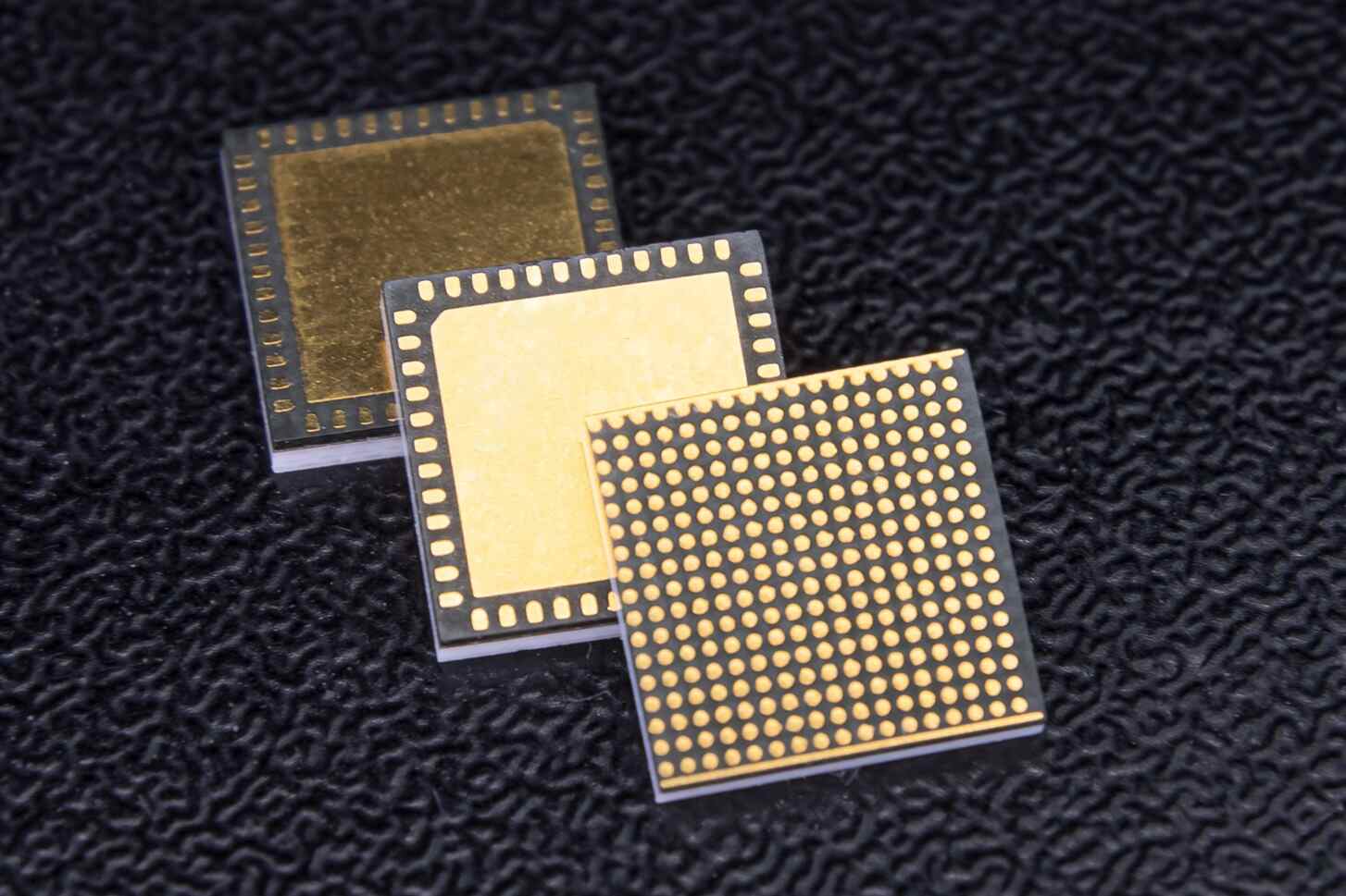
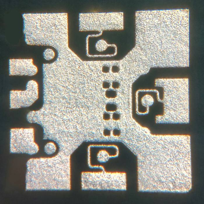
Flip Chip, AKA Controlled Collapse Chip Connection (C4), is an advanced packaging technology whereby the chip is flipped upside-down and connected directly to the substrate using small solder bumps. Bumps serve as electrical and mechanical connections between the chip and the substrate. |
|
Bonding Types |
Two main types of Wire Bonding: · Ball Bonding: Process typically uses gold wire. A small ball is formed at the end of the wire and attached to the bond pad using heat and pressure. The other end of the wire is then connected to the chip package using ultrasonic energy. · Wedge Bonding: Process often uses aluminum wire. The wire is threaded through a capillary and pressed against the bond pad without forming a ball. It can be done at room temperature. |
Types of Flip Chip Bumping: There are numerous methods that can be used in creating the solder bumps on Flip Chips:
|
|
Bonding |
Wire Bonding process key steps:
|
Flip Chip process key steps:
Underfilling the space between the chip and substrate for mechanical stability. Underfill materials are adhesives that are introduced between the flip-chip die and the substrate. They are configured to match the CTE of interconnect and distribute the stresses on interconnect solder joints. |
|
Advantages |
Advantages of Wire Bonding:
|
Advantages of Flip Chip:
|
|
Challenges |
Challenges of Wire Bonding:
|
Challenges of Flip Chip:
|
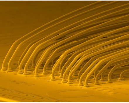
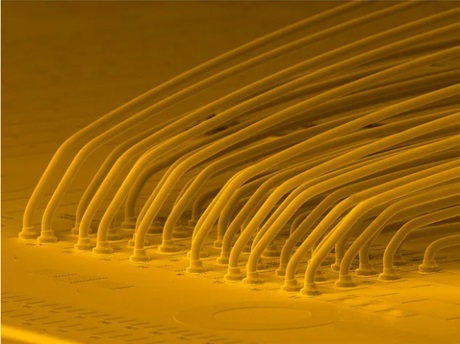
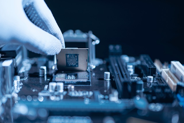
Figure 1: Wirebond wires in packages. Source: K&S
PERFORMANCE & OPTIMIZATION COMPARISON:
Electrical Performance: Flip Chip technology generally offers the superior electrical performance option due to its shorter interconnection lengths. This results in lower parasitic resistance, inductance, and capacitance.
Wire Bonding, while not as efficient, can still achieve good performance for many applications, especially when using design recommendations such as:
-
- Identifying and optimizing critical signals
- Paying careful attention to die pad ring design and placement
- Selecting the most suitable wire bond diameter
- Optimizing substrate signal path connectivity
Thermal Performance: Flip Chip packages typically have better thermal performance due to the direct contact between chip and substrate. However, wire bonded packages can improve upon thermal performance by implementing the following:
-
- Adding a thermal ball matrix in BGA packages
- Increasing the substrate layer count
- Maximizing the via count on the die attach pad
- Beefing up copper plane thickness
- Employing heatsinks, slugs, etc.
- Utilizing filled vias
Size & Density: Flip Chip technology allows for higher I/O density and smaller package sizes. Wire Bonding requires more space due to the need for bond pads around the chip periphery and the arc of the wire bonds. However, Wire Bonding can still achieve high density in some applications through techniques like staggered bond pad arrangements.
Cost Considerations: A cost comparison between Wire Bonding and Flip Chip technology is not straight-forward. Cost comparisons can be heavily influenced by type of application, case-specific issues, and additional factors such as:
-
- Die & wafer-level issues (e.g., bond pad pitch, configuration)
- Die cost & yield
- Type of Flip Chip bumping technology used
- Package assembly flow
- Process Total-Cost-of-Ownership (TCO)
- Production volumes
Costing Overview: Wire Bonding seems the more cost-effective method for lower I/O counts and lower production volumes. In non-leading-edge applications, Wire Bonding is considered the more cost-effective of the two IC packaging interconnect solutions. However, Flip Chip technology becomes more the more economical option when I/O count increases and for higher production volumes; mainly due to its smaller die area, that allows for more dies per wafer at a reduced cost per unit.
Manufacturability: When it comes to manufacturing process compatibility and ease of assembly, Wire Bonding remains the more flexible option, allowing for fewer complex design changes and faster turnaround times. Flip Chip requires more precise alignment and involves a more complex assembly process. However, in high-volume production, Flip Chip is more advantageous due to its potential for increased productivity.
Reliability: When properly implemented, both technologies can achieve high reliability. Wire Bonding boasts an established history of proven reliability for a wide range of applications. Flip Chip however provides outstanding reliability, particularly in harsh environments, due to shorter interconnects and underfill. Underfills are used for mechanical stabilization and protection, compensating for material stresses and reducing coefficient of thermal expansion (CTE), in electronic assemblies, especially Flip Chips.
At a Glance Comparison:
|
Feature |
Flip Chip |
Wire Bond |
|
I/O Density |
Higher I/O density, allows smaller, more compact chip packages, resulting in increased functionality. |
Lower I/O density, requires larger chip package sizes, with lower functionality. |
|
Interconnect |
Shorter interconnect lengths allow better electrical performance and lower ‘parasitic’ or (stray capacitance). |
Longer, thinner interconnect lengths due to wires, result in less effective electrical performance and higher ‘parasitic’ or (stray capacitance). |
|
Heat Dissipation |
Improved heat dissipation, reduces the risk of overheating. |
Less effective heat dissipation due to limited surface area for heat transfer. |
|
Package Size |
Smaller chip packages, allows for smaller electronic devices. Vertical stacking and 3D IC integration are easily achieved. |
Wires between chip and bond pad can be longer, resulting in a larger footprint. Vertical stacking is far more complex. |
|
Design |
More design complexity due to higher interconnection density. Requires precise alignment of pitch pads and solder bumps. |
Simpler design due to fewer I/O connections and less precision needed to attach wires to the bond pads. |
|
Costing |
At high volume and high manufacturing yields flip-chip can be more cost effective. The smaller die area fits more dies per wafer, reducing cost per unit. |
For non-leading-edge applications Wire Bonding is the most likely cost-effective packaging solution. |
|
Process Nodes |
Can be used for advanced process nodes in the rage of 7nm / 5nm. |
Can be used for more mature process nodes, in the rage 28nm / 14nm. |
USE-CASES & APPLICATIONS
Common Wire Bonding Applications: This basic technique is widely used in microelectronic products for a wide range of industries and applications, mainly because of its cost-efficiency, versatility and reliability:
-
- Integrated Circuits (ICs): Wire Bonding is still the dominant technology used in connecting IC chips to packages, especially for mature process nodes (28nm and above).
- Sensors: Many sensory devices, such as pressure sensors, temperature sensors, and accelerometers, use Wire Bonding for electrical connections.
- Optoelectronics: Devices like LEDs, photodiodes, and laser diodes regularly use Wire Bonding for electrical and optical signal transmission connections.
- Power Devices: MOSFETs and insulated gate bipolar transistors (IGBTs) frequently use Wire Bonding for power connections.
- Memory Devices: Many memory chips, especially those not requiring super high performance, use Wire Bonding.
Common Flip Chip Applications: In answer to market demand for quality high-speed and high-performance package design, the most commonly used packaging solution for these more advanced applications is flip chip technology:
-
- High-Performance Processors: CPUs and GPUs for computers and servers require Flip Chip technology to achieve the highest performance and I/O density.
- Advanced Mobile Devices: Smartphones and tablets increasingly use Flip Chip technology in their main processors and other high-performance components.
- Networking Equipment: High-speed routers and switches need the kind of improved electrical performance Flip Chip packaging can deliver.
- Automotive Electronics: Advanced driver assistance systems (ADAS) and other high-performance automotive electronics are readily adopting Flip Chip technology. See also: Automotive PCBs
- High-Frequency RF Devices: The shorter interconnects in Flip Chip technology make it an ideal solution for high-frequency applications in wireless communications.
EYE ON THE FUTURE
Monitoring Future Trends: Both Wire Bonding and Flip Chip continue to evolve, with a view towards meet pressing market demand for vastly improved near-future electronic device technology.
|
Wire Bonding Trends |
Flip Chip Trends |
|
|
Final Thoughts: The choice between Wire Bonding and Flip Chip depends on various factors, including electrical and thermal requirements, size constraints, production volume, and cost considerations. As the electronics industry continues to demand higher performance and smaller form factors, both technologies will likely coexist, with each finding its niche in different applications and market segments.
We hope you’ve found this blog article useful.
PLEASE FOLLOW OUR iNPACK PAGE on LinkedIn to see more blogs designed to bring you quality IC Packaging Technology subject matter. WE’D LIKE TO HEAR FROM YOU… Is there something in particular, you’d like to read about? Let us know.
About iNPACKTM
At iNPACK, we provide IC packages in a complex array of shapes, sizes, and materials, giving you the ability to select the exact features and functionality best suited to your specific application. This determination however is dependent upon a number of factors, including: Pitch, Dimensions, Lead Count, Thermal Requirements, Costing and more.
Contact us anytime to ask questions or discuss your next project.
Meet us at the IMAPS 2024 conference.