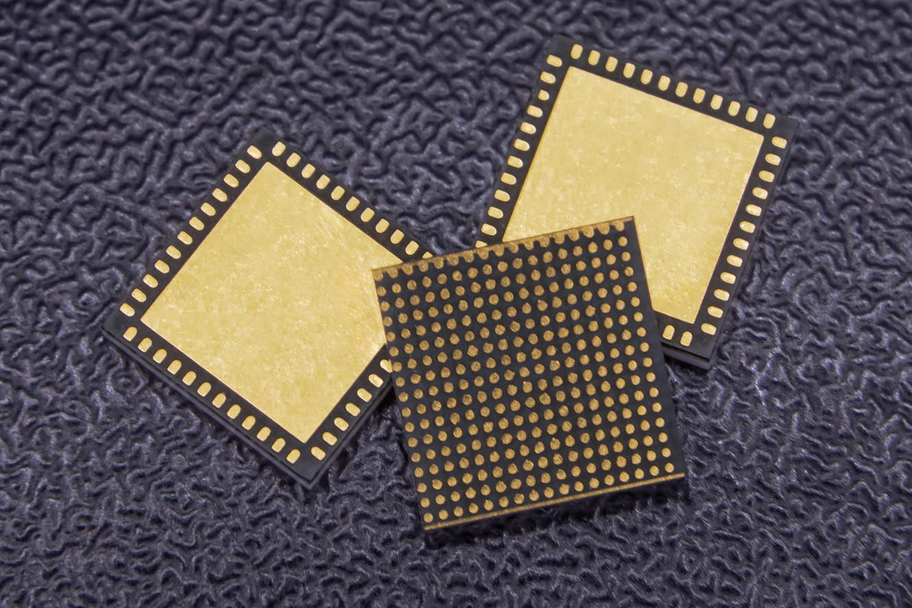
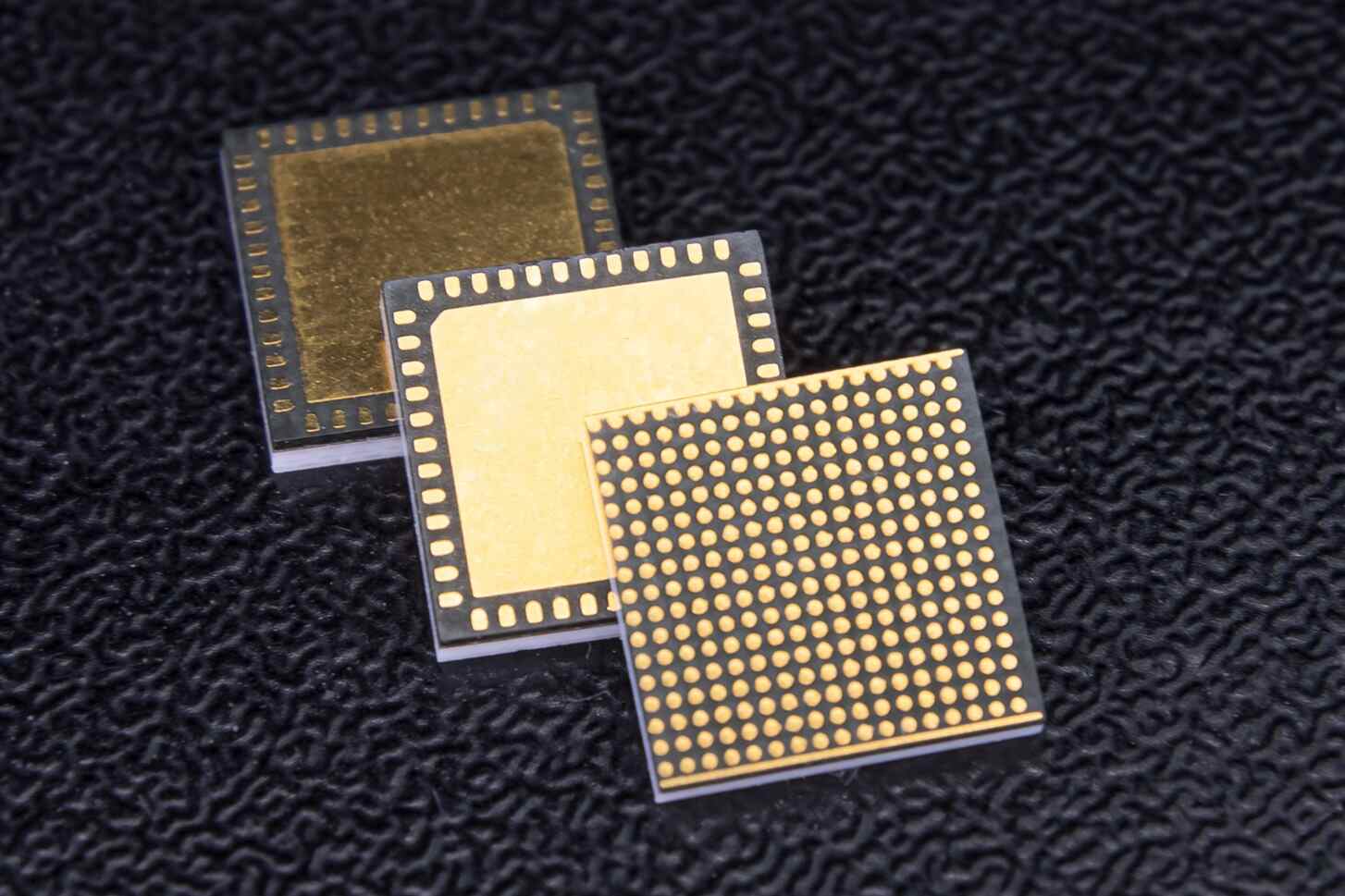
Panel-Level Packaging vs. Wafer-Level Packaging

Yaniv Meydar
|9th January ,2025
Unpacking the Future of Advanced Semiconductor Solutions with iNPACK
In the fast-paced world of electronics, miniaturization, cost-efficiency, and performance optimization are critical. Advanced packaging technologies—Panel-Level Packaging (PLP) and Wafer-Level Packaging (WLP)—are driving this evolution. Choosing the right approach significantly impacts production efficiency, scalability, and cost. With its expertise in panel-level solutions, iNPACK offers a distinct advantage.
Panel-Level Packaging (PLP): Efficiency at Scale
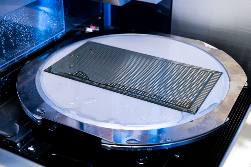
Panel-Level Packaging (PLP) utilizes rectangular panels similar to organic substrate manufacturing, designed specifically for high-volume production. This innovative approach boosts efficiency, reduces costs, and introduces the flexibility of MCM/SiP assembly. By leveraging a simplified process, working with known good dies, and optimizing product functionality with the best available technology for each required function, PLP delivers exceptional performance and value.
Key Advantages:
-
- Enhanced batch yields with rectangular panels, minimizing material waste.
- Tested and verified known good dies, leading to improved production yield.
- Supports advanced designs, including System-in-Package (SiP) and heterogeneous integration solutions.
- Highly cost-effective for industries such as automotive and aerospace systems.
- Incorporates 3D design options and integrates passive components for added functionality.
Wafer-Level Packaging (WLP): Precision and Form factor driven
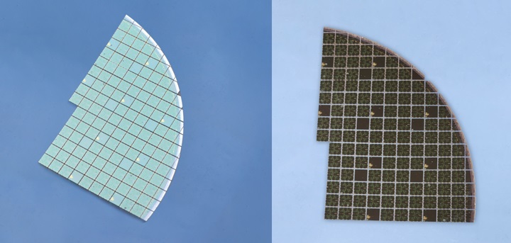
WLP involves packaging semiconductor dies directly on the wafer before dicing. This streamlined process supports fan-in designs, reduces handling and enables smaller form factors.
Key Applications of Wafer-Level Packaging :
-
- Ideal for compact devices including single-die RF and digital components.
- Facilitates mass production by bypassing substrate design and directly using RDL layers
Key Advantages:
-
- Reduces form factor
- Minimizes Production handling
- Provides an advanced Chip-Scale Packaging (CSP) solution
Limitations:
-
- Scalability is restricted by the wafer circular dimensions.
- Primarily supports single-die solution
Wafer-Level Packaging Structure:
Comprehensive Comparison Table
|
Feature |
Panel-Level Packaging |
Wafer-Level Packaging |
|
Process overview |
Processes multi chips on a panel |
Processes a single chip on wafers |
|
Form factor |
Rectangular or square panels |
Circular wafers |
|
Cost efficiency |
High volume for SiP |
High volume for single-die |
|
Production volume capability |
Scales well in mass production |
Limited scalability due to wafer size |
|
Manufacturing flexibility |
Supports diverse design needs |
Best for compact device designs |
|
Size limitation |
Accommodates large substrates |
Constrained by wafer diameter |
|
Typical applications |
Automotive, aerospace, consumer electronics |
Automotive, aerospace, consumer electronics |
|
Time to market |
Faster for SiP designs |
Faster for prototypes and high-volumes single-die |
|
Quality & reliability |
High with advanced penalization techniques |
Limited by chip yield |
|
Equipment requirements |
Requires specialized panel tools |
Relies on existing fab capabilities |
Applications and Innovation: Where PLP Excels
Panel-Level Packaging is the go-to choice for industries that require both high-volume production and advanced design flexibility:
-
- Automotive: Supporting advanced systems for connectivity, performance, and safety.
- Medical Devices: Ensuring compact, life-critical electronics like wearables and monitoring tools are reliable.
- Consumer Electronics: Powering miniaturized, high-performance devices for next-gen technologies like smartphones and IoT components.

iNPACK’s Panel-level Solution
iNPACK redefines production efficiency with its panel-level packaging solutions:
-
- Panel Processing: Supports 100×200 mm² panels for large-scale, efficient production.
- Substrate Solutions: Solve thermal expansion mismatches and signal integrity challenges.
- SiP Expertise: Integrates SMT, micro assemblies, and 3D interconnects to achieve compact, functional designs.
- Precision Manufacturing: Achieves 25µm lines and spacing to meet next-gen miniaturization standards.
- Quick Turnaround: Streamlined design-to-production reduces time-to-market without sacrificing quality.
iNPACK: Your Innovation Partner
iNPACK delivers advanced packaging solutions that optimize manufacturing processes, reduce costs, and drive next-generation designs to market.
Ready to transform your packaging capabilities?
Contact iNPACK today and discover how our Panel-Level Packaging solutions can revolutionize your production processes and fuel your innovation.

