QFN IC Packages | Panel Level Process for Organic Types

Yaniv Maydar
|20th August ,2024
PART ONE of our three-part blog series on:
Understanding Organic QFN IC Packages: Features & Applications
General Definition & Description of Organic QFN Packages
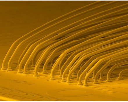
The QFN (Quad Flat No-lead) package is a versatile and efficient packaging technology widely used in various industries for very obvious reasons: low cost, small form factor, plus good electrical and thermal performance. Main components of QFN IC packages are a lead frame, single or multiple dies, wire bonds and molding compounds.
The organic QFN package uses organic materials as its substrate or base material. Today, organic substrates have overtaken the ceramics market due to their finer line and space capabilities, better heat management solutions and added flexibility to the design. Organic rigid substrates are classified into two categories: Laminate and Build-Up Types.
Key Characteristics & Features of Organic QFN IC Packages:
QFN Package types offer good performance, cost-effectiveness and manufacturability suitable for a wide range of electronic applications.
1. Substrate Material: Organic QFN packages typically use organic materials such as epoxy resin or laminate substrates as the base material. These materials are commonly used in standard PCB (Printed Circuit Board) manufacturing processes.
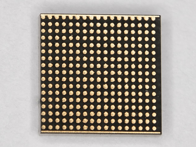
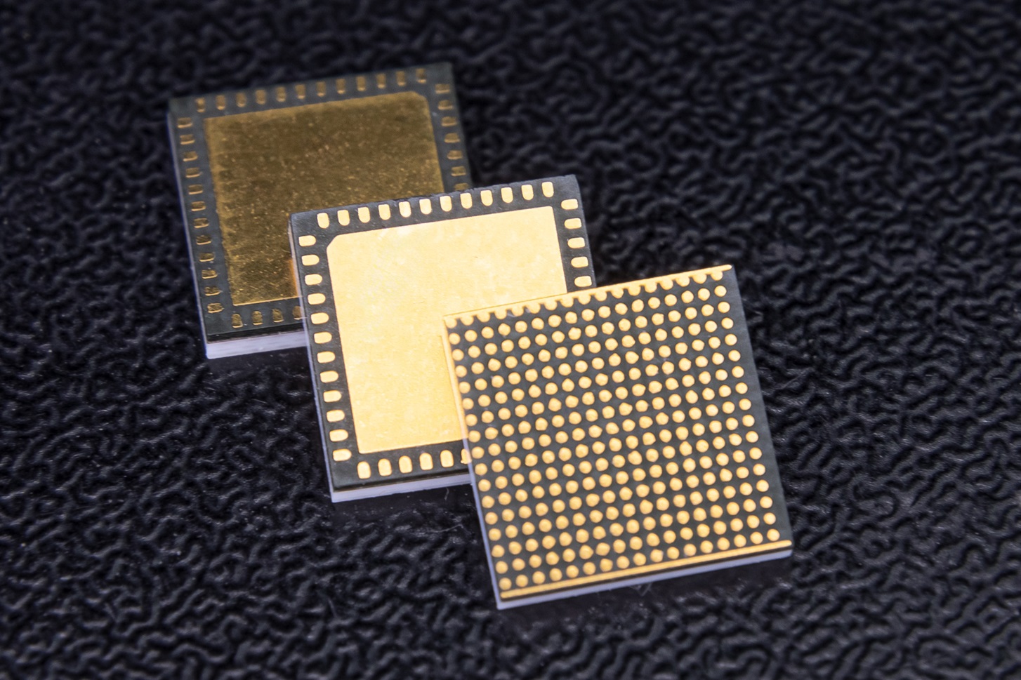
2. I/O Design: Like other QFN packages, organic QFNs have a pad IOs design where the semiconductor die is attached to a center pad structure. The signal IOs are arranged in a grid pattern around the periphery of the package.
3. No Leads: QFN packages are characterized by their leadless design, where the electrical connections are made directly from the IC packages pads to the PCB pads through solder joints on the bottom surface of the package.
4. Cost-Effective: Organic QFN packages are generally more cost-effective compared to other materials such as ceramic, due to the lower cost of organic substrates and their compatibility with standard PCB manufacturing processes.
5. Electrical & Thermal Performance: The electrical performance of organic QFN packages is typically adequate for a wide range of applications. They provide good signal integrity and thermal dissipation properties suitable for various electronic devices and systems.
6. Manufacturing & Assembly: Organic QFN packages are compatible with standard surface-mount assembly processes, including solder paste deposition and reflow soldering. This compatibility facilitates efficient and reliable manufacturing of electronic assemblies.
7. Applications: Organic QFN packages are commonly used in consumer electronics, telecommunications equipment, networking devices and additional applications where compact size, cost-efficiency and adequate performance levels are required.
Key Advantages of the QFN Package
• Packages are lightweight and easy to handle
• Packages are available with a thin profile & small form factor
• Short bond wires are used to connect die and frame
• Lead inductance of the QFN package is low
• Ideal for applications that require good heat dissipation
• Packages are easily available at a low cost
PROs & CONs of the QFN IC Package
• QFN solutions can offer a wide range of options to the designer
• The use of organic materials enables numerous material choices
• Control of CTE, DK, DF and even process-related properties such as TG
The combination of the right properties will lead to a robust design, however QFN challenges should also be taken into consideration.
|
Features |
PROs |
Features |
CONs |
|
Size & Weight |
QFN packages are compact and have a low profile compared to other packages like DIP (Dual In-line Package) or even SOIC (Small Outline Integrated Circuit), which helps in reducing the overall size and weight of the circuit board. |
Assembly |
QFN packages are challenging to solder manually due to the absence of leads. Proper soldering techniques, equipment, and skills are required to prevent solder bridging or inadequate connections. |
|
Thermal Performance |
The exposed pad on the underside of QFN packages helps in better thermal dissipation, making them suitable for high-power applications. This feature allows heat to be conducted away from the IC more efficiently. |
Inspection |
Visual inspection of solder joints can be difficult due to the package design, which may necessitate additional inspection methods such as X-rays, to ensure quality. |
|
Electrical Performance |
QFN packages generally offer good electrical performance due to shorter lead lengths and reduced parasitic inductance and capacitance compared to other package types. |
Mechanical Stress |
Because QFN packages are typically mounted directly onto the PCB with no flexible leads, they may be more susceptible to mechanical stresses during thermal cycling, resulting in solder joint failures. |
|
RF Performance |
The absence of leads and shorter interconnections can lead to lower parasitic elements, which is beneficial for high-frequency RF applications. |
Testing Accessibility |
Testing individual pins or connections on QFN packages can be difficult compared to packages with exposed leads, and may complicate debugging and testing processes. |
|
Cost Efficiency |
QFN packages are often less expensive than more complex packages like BGAs (Ball Grid Arrays) because of their simpler design and fewer materials. |
Repairability |
The need to replace a QFN package due to a fault or failure can be challenging, as it may require the use of specialized tools and techniques. |
Standards & Guidelines
Designing QFN (Quad Flat No-leads) packages or using components in QFN packages according to existing industry Standards & Guidelines, is critical in order to ensure proper functionality, reliability and manufacturability. When designing with QFN packages, engineers should refer to these Standards & Guidelines to ensure they’re meeting industry best practices.
1. JEDEC Standards:
JEDEC MO-220: This standard specifies the outline and dimensions of QFN packages, including lead pitch, pad layout and overall package dimensions. It defines various package sizes and configurations that manufacturers should adhere to.
JEDEC JESD51-12: Thermal characterization of semiconductor packages – User Guide.
2. IPC Standards:
IPC-7351: Generic Requirements for Surface Mount Design and Land Pattern Standard. This standard provides guidelines for the design of land patterns (footprints) for surface-mounted components, including QFN packages. It specifies dimensions and tolerances for pads and solder mask openings.
IPC-2221: Generic Standard on Printed Board Design. This standard provides guidelines for the design of printed circuit boards (PCBs), including considerations for mounting surface-mounted components like QFN packages.
3. Manufacturing Guidelines:
Design for Manufacturability (DFM): While not a specific standard, DFM principles are crucial in QFN design to ensure that the package can be manufactured with high yield and reliability. This includes considerations for solder mask, pad dimensions and thermal management.
4. Thermal Management:
QFN packages often have exposed thermal pads underneath the package, and it’s important to consider thermal vias, pad size, and layout to ensure effective heat dissipation. Standards like JEDEC JESD51-12 provide guidance on thermal characterization and management.
5. Electrical Design:
Ensuring proper electrical connections, signal integrity, and power distribution within the QFN package is critical. IPC standards and manufacturer datasheets provide guidelines on trace width, impedance control and signal routing for QFN packages.
6. Reliability & Testing:
Standards such as IPC-A-610 outline criteria for the acceptance of electronic assemblies, including requirements for soldering and mechanical assembly, which are important in ensuring the reliability of QFN packages.
7. Specific Manufacturer Recommendations:
Different semiconductor manufacturers may have specific guidelines and recommendations for the design and handling of their QFN packages. These can be found in datasheets and application notes provided by the manufacturer.
This concludes PART ONE of our three-part blog series: QFN IC Packages | Panel Level Process for Organic Types – iNPACK. We hope you found it useful.
Don’t miss PART TWO in this series: Get ready to explore QFN Package Types compared with LGA (Land Grid Array) and Other Packaging Options. Here you’ll find important information all in one place: Pros & Cons, Characteristics & Applications, plus a detailed comparison of critical features between QFN & LGA. Also presenting an overview of Ceramic vs. Organic vs Lead Frame QFN Options.
About iNPACK
At iNPACK (a PCB Technologies Company), we provide IC packages in a complex array of shapes, sizes, and materials, giving you the ability to select the exact features and functionality best suited to your specific application. This determination however is dependent upon a number of factors, including: Pitch, Dimensions, Lead Count, Thermal Requirements and Costing.
The QFN (Quad Flat No Lead), represents a specific IC Packaging solution. iNPACK offers a customized panel-level solution featuring a plastic-encapsulated laminate panel, with a variety of dielectric and CTE options for electrical interconnection with the PCB. This type of packaging can be offered as a full turn-key solution, (including assembly and testing), or as a stand-alone substrate, combined with a cavity lid.