Antenna-In-Package (AiP) Solutions: The Time is Now
Yaniv Maydar
|6th November ,2024
RF system designers know, the need is critical! They must re-evaluate all components in the signal chain in order to reduce size, weight, power, and cost, while increasing or at least maintaining current performance levels. They have little choice but to economize and innovate now.
For the right applications and functionality, AiP technology can provide a superior solution, offering advantages in reduced size and weight, fewer components and assembly steps, optimized performance levels and greater design flexibility. AiP systems are found in a wide variety of applications and industries including: Mobile phones, WiFi routers, wireless sensor networks, automotive radar, drone PCBs, military & defense equipment, medical imaging, wearables and more.
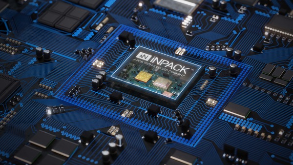
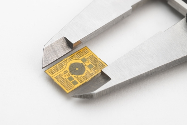
AiP Configuration: The Antenna-in-Package modality implements one or more antennas in an IC-type package along with a bare RF chip transceiver. It has ability to integrate additional front-end components such as power amplifiers or low-noise amplifiers, switches, filters, and power management integrated circuits using System in Package (SiP) technology. The packaging process utilizes double-sided molding, selective molding, passive component integration, and various EMI shielding methodologies.
AiP design commonly uses a flip-chip ball grid array with an RF chip (transceiver) attached to a package substrate with solder balls for connection to the main PCB. An antenna, or even an array of antennas, sits atop the package substrate, allowing wireless communication and detection. The Flip-chip connects the RF chip to the substrate, minimizing interconnect loss. The overall AiP configuration can simplify challenges associated with mmWave applications, while also helping to speed up the design process.

General Advantages of Antenna-In-Package (AiP)
- Improved thermal performance; dissipates heat more efficiently than conventional systems — extending system longevity
- More resilient to harsh environmental factors such as moisture and heat
- Design provides higher security levels against unauthorized access or tampering
Optimization: The benefits of implementing the antenna and RF chip (transceiver) in a single package, instead of having the antenna as a separate component placed on or near the system PCB, includes:
- Shorter interconnection between the antenna and RF chip
- Enhanced signal integrity and reduced signal attenuation
- Reduced range and propagation challenges at higher frequencies
- Competitive edge resulting from a smaller form factor (SFF)
AiP Operating Range
Suitable Frequencies & Wavelengths: Wavelengths and related antenna sizes dimensionally compatible with AiP and IC-type package sizes: 1 GHz, electromagnetic wavelength (λ) — 0.3 meters; at 10 GHz — 0.03 meters (3 cm/30 mm); and at 100 GHz — 0.003 meters (3 mm).
Frequencies That Fit: Owing to physical wavelength issues, the option offering the optimal fit is the millimeter wave (mmWave) spectrum; with wavelengths between 10 millimeters (30 GHz) and 1 millimeter (300 GHz), referred to as the extremely high frequency (EHF) band. However, AiP activity in the 1 to 30 GHz range is also not uncommon.
Swift Adoption of AiP:
AiP technology is widely used in high-frequency applications such as 60-GHz radios and gesture radar, 77-GHz automotive radar, 94-GHz phased arrays, 122-GHz imaging sensors, 300-GHz wireless links and for 5G mobile networks operating at mmWave frequencies such as 28, 39, 60, 77, 90 GHz and beyond.

The 5G Influence: Because of significantly smaller antennas at mmWave frequencies of 5G devices, the antenna in the mmWave band can be directly integrated in the package. In addition, the multiple antennas needed by some 5G designs for ‘multiple in/multiple out’ diversity antenna configurations, are a good fit for AiP.
Are There Limitations to AiP? The technology may not be suitable for all RF designs. Keep in mind that because the RF components and antenna elements must be modeled as a single unit, not individually, special efforts in up-front design, planning, and implementation are necessary. Consideration with respect to frequencies, thermal issues, RF power, DC power, and other design aspects must be factored in as well. Please feel free to consult with our experts at PCB Technologies about your RF design needs.
In Conclusion: Antenna-in-Package technology
Under certain conditions, Antenna-in-Package technology is a preferred approach to the challenges of higher RF integration, especially (but not limited to) frequencies above 10 GHz. PCB Technologies pass on to our customers the highest level of expertise in PCB and PCBA design and fabrication, implemented for custom miniaturization solutions.
iNPACK offers a wide range of In-Package systems for high-frequency applications: From 60 GHz for radio, automotive radar, phased arrays, advanced sensors etc., and from 20 GHz up to 100 GHz for special applications. Have a question? Get in touch with one of our experts about your AiP design needs now.


