All-in-One Substrates and Advanced Packaging Solutions
VARDIT HARZMAN
|4th August ,2022
Since it is not just critical that any electronic device works correctly in tests, but also essential that the device continues to work at full performance and accuracy, even for decades, in the customer’s application. In a specific case, an overall solution was required to tackle this comprehensive challenge and assure no detail goes unnoticed. We, at PCB Technologies, have realized, based on long years of experience, that by providing the manufacturing designer with a full PDK (process design kit) and integration, we can get a reliable and quality product that is efficient on a smaller form factor. The meaning of this is that we can combine the constraints of the manufacturers and avoid manufacturing failures. When design and manufacturing teams work hand-in-hand, implying there is little or no time to do heavy pre-characterizations, the advantage of an All-in-One PDK is best materialized.
This way designers can now plan and manage their package design intent across all their components using tools. The verification tool allows package designers to verify the connectivity of the post-package design against the design intent.
What does all this mean?
We not only need EDA tools, but also a design ecosystem. Processes, tools, and requirements must all come together in a well-established and trusted design flow embodied by the PDK. In the end, the PDK is the element that bridges the gap between diverse design teams and manufacturers to drive the future of technology.
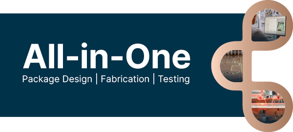
At PCB Technologies we combine package design, board and organic substrate fabrication, testing, and assembly technology processes, all under the same roof. Our goal is to work with customers at the very beginning of their design; this is the best way to help them miniaturize their systems, upgrade their performance and simplify their integration
The design process is an All-in-One process, because you can both design the PCB board, the substrates, and the packaging solution at the same location while utilizing unified design rules which can later on be implemented at the fabrication and testing stages. This saves the need for moving between subcontractors when solving your problem and planning ahead the production and testing processes.
Integration is the key factor here and it’s especially useful in tailor-made products, not off-the-shelf ones. The whole process is dedicated to solving specific requirements based on the customer’s needs.
If, for example, a customer has already designed their package, but they need the substrate board to come into play, we can support them design the substrate for any problem they might have. We can dissolve thermal dissipation concerns with a coin insert or any other solution that can draw the heat out the backside.
In conclusion, if you want to get a high-reliability electronic device – it’s best if your DFX (design for excellence) is carried out by one engineering team for the PCB design and manufacturing, assembly, and complete system integration, thus allowing the planning and execution of the optimal tests and inspections necessary for the product’s design, quality, cost-effectiveness, and functionality.