Talk to an Expert

LET'S TALK

IC Packaging

Think miniaturization, think iNPACKâ„¢

IC Packaging Capabilities

Welcome to a wealth of information about IC Packaging, from the basic to the complex. This includes definitions, related terms, an outline of various IC package types, their relative advantages & challenges, comparison tables, plus key takeaways.

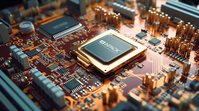
We provide IC packages in a complex array of shapes, sizes, and materials, giving you the ability to select the exact features and functionality best suited to your specific application. This determination however is dependent upon a number of factors, including: Pitch, Dimensions, Lead Count, Thermal Requirements and Costing.

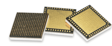
QFN (Quad Flat No Lead), represents a specific IC Packaging solution. iNPACK offers a customized panel-level solution featuring a plastic-encapsulated laminate panel, with a variety of dielectric and CTE options for electrical interconnection with the PCB. This type of packaging can be offered as a full turn-key solution, (including assembly and testing), or as a stand-alone substrate, combined with cavity lid.

10 Useful IC Packaging Definitions & Terms

  • Abbreviations

    Names of various IC package types: DIP, SIP, SOP, SSOP, TSOP, MSOP, QSOP, SOIC, QFP, TQFP, BGA, etc.

  • Interposer

    Made of silicon, glass, ceramic or organic materials, the interposer functions as a bridge between multiple dies, dies and the PCB. Used in multi-chip die or boards, to pass electrical signals through in a package.

  • TSV (Through-Silicon Via)

    It is a type of VIA (Vertical Interconnect Access) connection, that creates vertical electrical connections between silicon wafers or dies.

  • System-on-Chip (SoC)

    Type of integrated circuit (IC) design combining multiple high-level electronic device functionality elements onto a single chip in place of separate components mounted to a board.

  • System-in-Package (SiP)

    Involves numerous integrated circuits (ICs) enclosed in one chip package. It can encompass an IC package substrate that includes passive components and is able to execute functions of an entire system.

  • 2.5D Packaging

    Where dies are stacked or placed side by side on top of an interposer based on TSVs.

  • 3D IC Packages

    Where logic dies are stacked on top of each other or memory dies, instead of creating a larger System-On-Chip (SoC). Dies are connected using an active interposer. A 3D IC package uses multiple layers of silicon wafers stacked together along with components using TSVs.

  • Fan Out

    Packages whereby connections are fanned out of the chip surface to facilitate more external Input/Output (I/O) circuits.

  • Fan-out Wafer-level Packaging (FOWLP)

    Makes way for more external contacts with silicon die. Considered an upgrade over wafer-level packaging (WLP).

  • Heterogeneous Integration

    Functions similarly to a system-in-package (SiP); however, it integrates multiple IPs as ‘Chiplets’ on a single substrate.

The Key Advantages of IC Packaging

There are numerous types of IC packages, each with its own strengths and challenges. IC Package types should be selected based on factors such as size, functionality and budget constraints. Choosing the optimal IC packaging design will ensure reliable functionality and high-performance levels for a wide range of electronic applications.

Main advantages include:

Protection

The IC package shields the chip from any possible physical harm by rough handling or droppage, causing parts displacement, breakage or excessive wear. It also protects against environmental threats that can adversely affect chip performance and reliability such as moisture, dust or corrosive agents.

Space Optimization

IC packaging allows for smaller form factor with increased functionality. Its significantly smaller size compared with using individual discrete components, enables more compact designs and increased component density on PCBs — a perfect solution for wearables and mobile devices.

Noise Reduction

The IC package design can help minimize electrical noise interference within the circuit, allowing more stable and reliable operation.

IP (Intellectual Property) Protection

The IC Package encasement literally protects designed components by incorporating registration and licensing information.

Electrical Connection

The package provides an efficient method of transferring the electrical signals within the chip to the outside world. It accomplishes this by incorporating electrical contacts, such as pins or pads, that allow the chip to connect to the PCB.

Ease of Assembly

IC Packaging facilitates easy and consistent automated component assembly, which in turn, reduces manufacturing costs and quality issues. This becomes an especially critical issue compared with components that require intensive soldering and other time-consuming processes.

Thermal Management

Some advanced packaging solutions incorporate features for improved heat dissipation, critical in high-performance ICs.

Main Types of IC Packaging Technologies

DIP = Dual In-Line Package

One of the oldest and simplest types of IC Packaging, with two rows of metal pins.

Advantages:

Easy to handle & solder

Challenges:

Relatively large, takes up precious space

SOP = Small Outline Package

A surface-mount package, soldered directly onto the PCB surface.

Advantages:

Space-efficient

Challenges:

Can be difficult to solder by hand

QFP = Quad Flat Package

A surface- mount package with pins on all four sides for higher pin count.

Advantages:

Higher pin count than SOP

Challenges:

Not suitable for high pin-count ICs, limited heat dissipation capability

BGA = Ball Grid Array

A surface-mount package with solder balls on the bottom, offering maximum connection density.

Advantages:

Highest connection density

Challenges:

Manufacturing, rework and maintenance is more challenging

Range of IC Packaging Design Formats

Below is a comprehensive list, with explanations, key features, applications and new developments pertaining to a wide range of IC Packaging Formats. Find the exact IC Packaging solution to meet your specific requirements:

LAMINATE

Definition:

Laminate packaging uses laminated substrates to house ICs. Constructed by stacking layers of thin laminate materials with double-sided copper foil, they offering excellent electrical performance and mechanical stability. High power / high-speed ICs needing enhanced electrical and thermal performance benefit from the higher functionality of laminate package technology.

Key Features:

  • High-frequency performance
  • Robust mechanical support
  • Good thermal management

Common Applications:

High-speed processors, telecommunications equipment, advanced computing systems.

Recent Developments:

Advances in new materials and manufacturing processes have helped to enhance performance while reducing costs of Laminate packaging.

LEADFRAME

Definition:

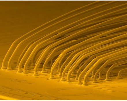
Leadframe packaging involves a metal frame that supports the IC and connects it to the external circuitry. Wiring from tiny electrical terminals on the surface of the semiconductor, are connected by a thin layer of metal to the large-scale circuitry on electrical devices or PCB.

Key Features:

  • Cost-effective
  • High-volume production
  • Simple design

Common Applications:

Consumer electronics, automotive components, power management devices.

Recent Developments:

Innovations in Leadframe design are helping to improve thermal performance and miniaturization capabilities.

MEMORY & STORAGE

Definition:

Integrating Memory & Storage in a single package, this IC packaging format is optimized for high-density memory chips, such as DRAM and flash memory.

Key Features:

  • High-density integration
  • Fast data access
  • Reliable performance

Common Applications:

Solid-state drives (SSDs), memory modules, and embedded storage solutions for mobile, computing and autonomous automotive technology.

Recent Developments:

The development of 3D NAND technology is revolutionizing memory packaging by increasing storage capacity and reducing costs.

MEMS & SENSORS

Definition:

MEMS (Micro-Electro-Mechanical Systems) and Sensor Packaging is designed for small, sensitive devices designed to detect physical, chemical, or biological changes in the environment.

Key Features:

  • Miniaturization
  • High sensitivity
  • Environmental protection

Common Applications:

Smartphones, medical devices, automotive sensors, authentication, wearable sensors.

Recent Developments:

The integration of MEMS with ICs is helping to enhance functionality while also reducing the size of the sensor packages.

POWER DISCRETE

Definition:

Power Discrete Packaging is used for individual semiconductor devices that need to handle high power levels. These power packages are optimized for power-sensitive and mobile applications, and feature innovative high-performance packaging capabilities.

Key Features:

  • Efficient heat dissipation
  • High reliability
  • Robust performance

Common Applications:

Power transistors, diodes and voltage regulators for wide array of applications in sectors such as automotive, communications and industrial.

Recent Developments:

New materials and packaging techniques are helping to improve efficiency and performance of Power Discrete Devices.

SYSTEM IN PACKAGE (SiP)

Definition:

System in Package (SiP) integrates multiple ICs and passive components into a single package. It’s an ideal solution for markets demanding a reduced footprint with increased functionality and higher levels of integration at lower costs.

Key Features:

  • High integration
  • Space-saving design
  • Enhanced functionality

Common Applications:

Aerospace & Defense Systems, Medical Devices, Data Center Processing.

Recent Developments:

SiP Technology is evolving to include increasingly complex, heterogeneous integration, in order to pack even more advanced functionality into ever-smaller, compact devices.

WAFER LEVEL PACKAGING

Definition:

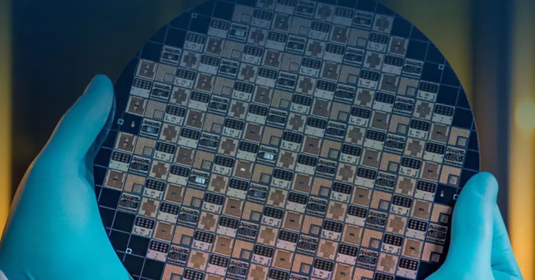
Wafer Level Packaging (WLP) involves packaging ICs while still on the wafer. This allows greater bandwidth, speed and reliability. Featuring a small form factor and high-performance levels, WLP technology is applicable for a wide range of semiconductor device types.

Key Features:

  • Reduced package size
  • Improved performance
  • Lower cost

Common Applications:

Mobile devices, high-frequency RF applications, compact electronic devices.

Recent Developments:

The development of fan-out WLP has greatly extended capabilities and applications for this type of IC packaging.

QFN

Definition:

Quad Flat No-Lead (QFN) packaging is a surface-mount technology that offers a small footprint and excellent thermal performance.

Key Features:

  • Compact size
  • Good thermal and electrical performance
  • Cost-effective

Common Applications:

RF modules, power management ICs, sensor devices.

Recent Developments:

Enhanced QFN designs are providing better performance and reliability for high-frequency applications.

ENCAPSULATION

Definition:

Encapsulation involves the process of encasing ICs in a protective material to shield them from harmful environmental factors. Potential sources of damage to dies include moisture, dust, dirt, solvents, mechanical stress and abrasion. Encapsulation deposits can consist of epoxy, sealants and other additives used individually or in combination.

Key Features:

  • Environmental protection
  • Mechanical stability
  • Enhanced durability

Common Applications:

Automotive electronics, industrial controls, and consumer electronics.

Recent Developments:

Advanced encapsulation materials and new techniques are improving reliability and lifespan of electronic devices.

RDL PACKAGING

Definition:

Redistribution Layer (RDL) Packaging adds additional layers of metal interconnects to the wafer. The wiring layer is formed of Cu (Copper) and an insulating layer. Commonly used in WLP Fan-Out or 2D packaging structures, its function is to connect the semiconductor chip to the board connector.

Key Features:

  • Complex routing capabilities
  • High-density interconnects
  • Improved performance

Common Applications:

Advanced computing, telecommunications, high-performance electronics.

Recent Developments:

Fan-out RDL Technology enables more complex and higher-density packaging solutions.

BGA

Definition:

Ball Grid Array (BGA) packaging, features an array of solder balls on the underside of the package, functioning as a surface-mount packaging for integrated circuits. BGA packages are used to permanently mount devices such as microprocessors. BGA packaging is a popular solution as it allows more interconnection pins than a dual in-line or flat package does. It is also a big space saver by utilizing fewer components and components with smaller footprints.

Key Features:

  • High-density interconnection
  • Good thermal and electrical performance
  • Robust mechanical support

Common Applications:

High-performance processors, graphics cards, networking equipment.

Recent Developments:

Innovation in BGA design helps improve thermal management and electrical performance.

FLIP CHIP PACKAGING

Definition:

Flip chip packaging involves flipping the IC and directly attaching it to the substrate or PCB using solder bumps. The Flip Chip allows for a large number of interconnects with shorter distances than wire, which greatly reduces inductance

Key Features:

  • Shorter electrical paths
  • Improved performance
  • Improved thermal management

Common Applications:

High-speed processors, graphics processors, advanced computing devices.

Recent Developments:

Advances in Flip Chip Technology have greatly enhanced its functionality for high-frequency /high-performance applications.

Summary of IC Package Design Formats

Packaging Type Key Features Common Applications Recent Developments
Laminate High-frequency performance, mechanical support High-speed processors, telecom Enhanced materials and processes
Leadframe Cost-effective, high-volume production Consumer electronics, automotive Improved thermal performance
Memory & Storage High-density, fast access SSDs, memory modules 3D NAND technology
MEMS & Sensors Miniaturization, high sensitivity Smartphones, medical devices Integration with ICs
Power Discrete Efficient heat dissipation, high reliability Power transistors, diodes New materials and techniques
System-in-Package (SiP) High integration, space-saving Smartphones, wearables Complex and heterogeneous integration
Wafer Level Packaging Reduced size, improved performance Mobile devices, RF applications Fan-out WLP
QFN Compact, good thermal performance RF modules, power management ICs Enhanced designs for high-frequency use
Encapsulation Environmental protection, mechanical stability Automotive, industrial controls Advanced materials and techniques
RDL Packaging Complex routing, 
high-density interconnects Advanced computing, telecom Fan-out RDL technology
BGA High-density, robust support Processors, graphics cards Improved thermal management
Flip Chip Packaging Shorter paths, improved performance High-speed processors, graphics Advances in high-frequency applications

IC Packaging Applications

Most commonly used IC Package applications according to industry / technology sectors:

HEALTHCARE

Applications:
Portable diagnostic equipment, wearable monitors, implantable devices, tele-health devices.


Relevant Certification:
ISO 13485 (Medical Devices Quality Management).

DEFENSE & AEROSPACE

Applications:
Avionics, radar systems, communications equipment.


Relevant Certification:
AS9100 (Aerospace Quality Management), MIL-STD-883 (Military Standard for Microcircuits).

AUTOMOTIVE

Applications:
Advanced Driver Assistance Systems (ADAS), in-vehicle infotainment systems, electric vehicle components.

WEARABLE DEVICES

Applications:
Fitness trackers, smartwatches, augmented-reality eyewear.


Relevant Certification:
ISO 9001 (Quality Management).

DRONES

Systems combining robotics with aeronautics

Applications:
Commercial drones, military UAVs, delivery drones.


Relevant Certification:
AS9100 (Aerospace Quality Management).

OPTICAL

Applications:
Optical transceivers, fiber-optic communications systems, LiDAR systems.


Relevant Certification:
ISO 9001 (Quality Management).

IC Packaging – Main Challenges

1. Thermal Management

Problem

Common Applications:
High-speed processors, telecommunications equipment, advanced computing systems.

Solution

The need to understand design considerations to reduce heat and the advanced cooling techniques available to boost heat dissipation. This includes micro-channel heat sinks, thermal-interface materials, integrated heat spreaders and more. To develop an effective thermal management strategy, see charts below.

2. Miniaturization & Integration

Problem

The demand for smaller, more densely integrated devices can seriously challenge our capabilities in maintaining performance levels while reducing size.

Solution

Utilizing 3D packaging technologies, such as Through-Silicon-Vias (TSVs) and System-in-Package (SiP) technology, enables better integration and increased functionality in compact footprints.

3. Reliability and Durability

Problem

IC Packages must continuously withstand mechanical, thermal and environmental stresses, without failure over their operational lifetime.

Solution

Utilization of robust materials, advanced encapsulation methods and rigorous testing protocols can help boost durability and reliability, ultimately increasing the lifespan of IC Packages.

4. Electrical Performance

Problem

To ensure high-speed signal transmission with low power loss in increasingly complex IC Packages is a real challenge.

Solution

Optimizing package design with low-loss materials, improving interconnect technology and utilizing simulation tools to validate electrical performance can help address these issues.

Design considerations for thermal solutions

  • Major heat-dissipating components
  • Board size and thickness
  • Materials, layout, & component placement
  • Mounting peripherals
  • Application conditions & environment
  • Amount of heat dissipated
  • Cooling methods, (fans, heat sinks, etc.)

Thermal management solutions available

  • Cu coins (I-coin, T-coin, custom-coin)
  • Heat sinks (soldered, deductive adhesive, non-conductive)
  • Thermal vias (Cu-filled, epoxy filled)
  • Cu thickness
  • Integrated active cooling designs
  • Specialized assembly solutions

Process & Machinery

SMT P&P

Curing (Flux-less Vacuum Soldering)

Laser Marketing / Labeling / Print

Reflow

Wedge & Ball

Dicing (Package Sawing)

XRAY

Plasma

Cross Section

Die Attach (soldering and adhesive)

Molding (Encapsulation)

QFN Package

Sintering

Through Mold Interconnection

Dispensing & Stamping

Laser Jet Ball (for BGA)

FAQ: Frequently Asked Questions 

1. What is the main purpose of IC Packaging?

The IC package serves a number of functions: To protect the delicate silicon chip inside it, to facilitate connecting the chip with other components on the printed circuit board, and to provide IP (Intellectual Property) protection for designed components used in fabricating semiconductor chips or ICs.

2. Why choose a Ball Grid Array (BGA) package?  

BGAs allow a high density of connections, suitable for high-performance devices which require a large number of pins; such as smartphones or gaming consoles.

3. What is a major challenge of IC Packaging design?

Balancing miniaturization with heat dissipation. Chips are becoming smaller in size yet more powerful, with increased functionality. Consequently, these tiny IC packages generate a great amount of heat, which requires implementing thermal management solutions.

4. Why is Signal Integrity a challenge in IC Packaging?

In very small packages with high clock speeds, electrical signals can create interference or crosstalk. Careful design and the use of advanced or composite materials can help improve and maintain signal integrity.

5. What is the trade-off between cost & performance in IC Packaging?

Complex packaging solutions using high-performance materials can be expensive. Every new IC device adds its own set of challenges, from smaller features and new materials, to the integration of discrete components. Finding a balance between cost, functionality, reliability and manufacturability is crucial. Consult with PCB manufacturing experts to discuss all the important considerations.

6. Why is IC Packaging design important?

The choice of package significantly impacts the final application. Smaller packages enable portable devices, while advanced packages support high-performance computing. Careful design is crucial in order to translate concepts into reliable, efficient and profitable electronic devices.

7. What is Wafer Level Packaging (WLP)?

Wafer Level Packaging (WLP) involves packaging the ICs while they are still part of the wafer, before being diced into individual chips. This method enhances performance and reduces the size and cost of the final package, making it ideal for mobile devices and high-frequency RF applications.

To get the file, fill in your Email

Thank you

We will contact you shortly